Getting Started
This section describes all the necessary steps to connect the Monocle Developer Board for firmware and FPGA development.
Setup
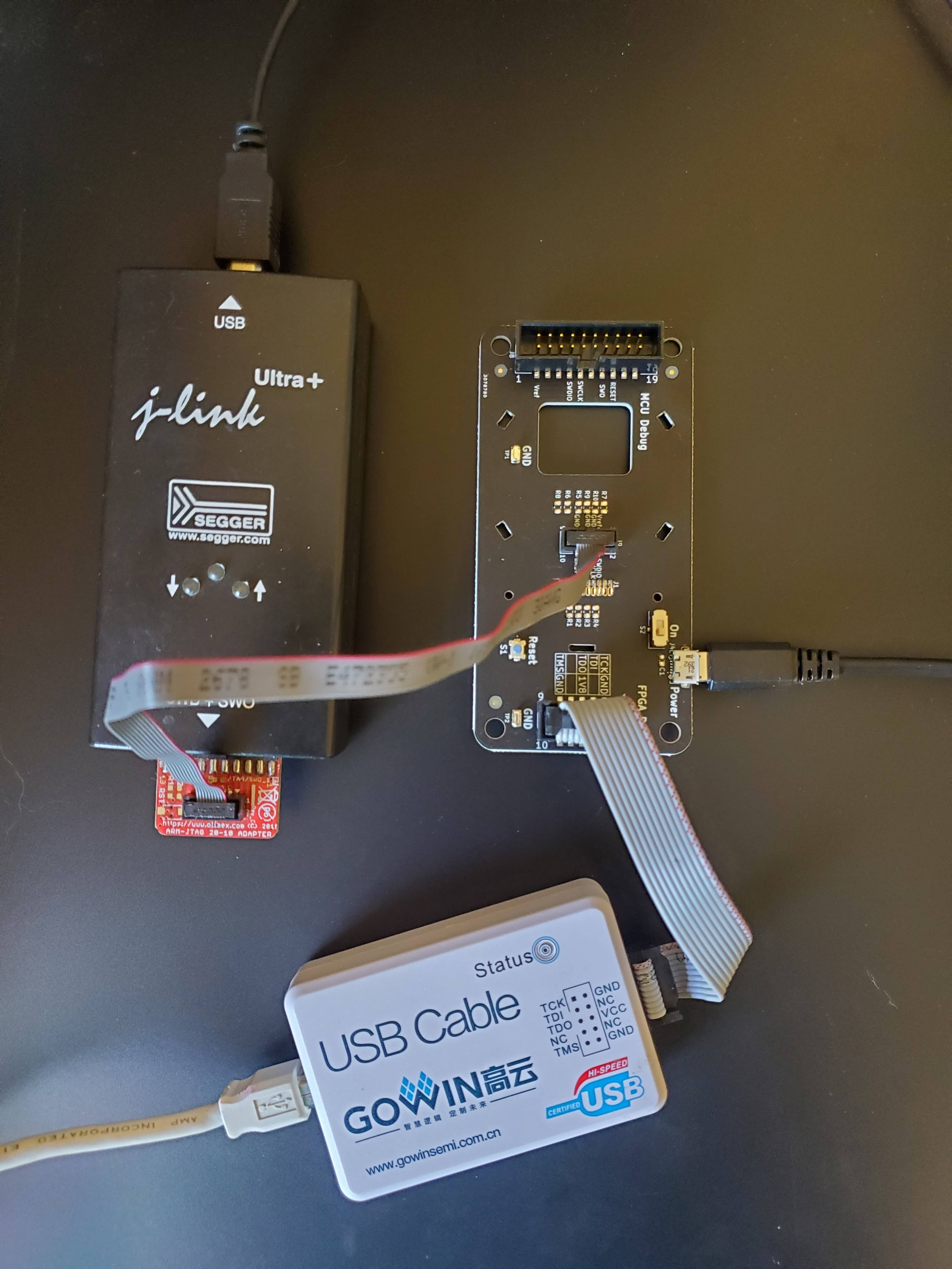
The picture above shows the various components connected to the Developer Board
Micro USB cable for power
JLink programmer required for firmware development/debug
Gowin programmer cable required for FPGA programming/debug
Note that the Developer board allows you to connect either a 10-pin JTAG/SWD cable or a larger 20-pin connector.
Suggested setups:
Firmware Developers: Any JTAG debugger that works with the Segger Embedded Studio would work well. A variety of JLink programmers have been found to work well.
FPGA Developers: You will most likely need to also do some firmware modifications if you decide to change the FPGA code so access to a SWD compatible programmer is highly recommended. In addition, you will need a Gowin programmer cable.
Troubleshooting
The firmware has a power-on self-test feature which checks that all hardware is correctly started-up.
After starting, the green LED turns on, then the peripheral are configured.
Then if anything failed, the red LED turns, and a report is shown by blinking the green LED.
For each failed peripheral, the green LED will blink a sequence of multiple blinks depending on which peripheral did fail. If it blinks 3 time in a row, then 4 times in a row, it means that the step 3 and 4 failed.
Then the red LED will stay up for a while, then turn off as the device reboots into bootloader mode. At this moment, you may flash a firmware image.
After a timeout of 15s without action, the bootloader will execute the main firmware once again. And start at the first step above once again.
Here is the reference for the green led blink report:
Init of
Maxim Integrated MAX77654PMIC and other GPIO signals.Init of
Azotec IQS620capacitive touch buttons controller.Init of
GoWin GW1NFPGA and its Verilog RTL circuit.Init of
Sony ECX336CNmicrodisplay.Init of
OmniVision OV5640camera module.Init of
OV5640Flash chip.